
Your Power Supply Works Perfectly—So Why Did It Fail EMC Testing
Date:2026-07-10 Publisher:BettpowerYour Power Supply Works Perfectly—So Why Did It Fail EMC Testing?
A Practical Guide to Finding EMI Sources and Improving EMC Performance in Switching Power Supplies
Introduction
Your power supply works.
The output voltage is stable.
Efficiency meets the design target.
Protection functions operate correctly.
The prototype appears ready for production.
Then the EMC test report arrives:
Failed.
Conducted emissions exceed the limit.
Radiated emissions are higher than expected.
The engineering team must return to the design stage.
This situation is common in switching power supply development.
A converter can achieve excellent electrical performance while still generating excessive electromagnetic interference (EMI).
The reason is that a power supply does not only transfer energy.
It also creates high-frequency electrical noise during switching operation.
The key challenge is not eliminating all noise.
It is controlling:
· Where noise is generated
· How noise travels
· How noise escapes from the system
This article provides a practical troubleshooting approach to help engineers identify EMI sources and improve EMC performance.
Part 1
Find the EMI Source
Why Does a Working Power Supply Fail EMC Testing?
Functional testing and EMC testing evaluate different aspects of a design.
Functional testing verifies:
· Output voltage stability
· Efficiency
· Protection functions
· Thermal performance
EMC testing evaluates:
· Electromagnetic emissions
· Noise propagation paths
· System compatibility
A power supply can pass all functional tests and still fail EMC because unwanted high-frequency energy is not properly controlled.
Quick Answer
Most EMC failures are related to:
· Large high-frequency current loops
· Poor EMI filter implementation
· Switching waveform ringing
· Transformer parasitic coupling
· Uncontrolled noise return paths
· Cable radiation
The first step is not adding more components.
The first step is:
Find where the noise is generated and how it travels.
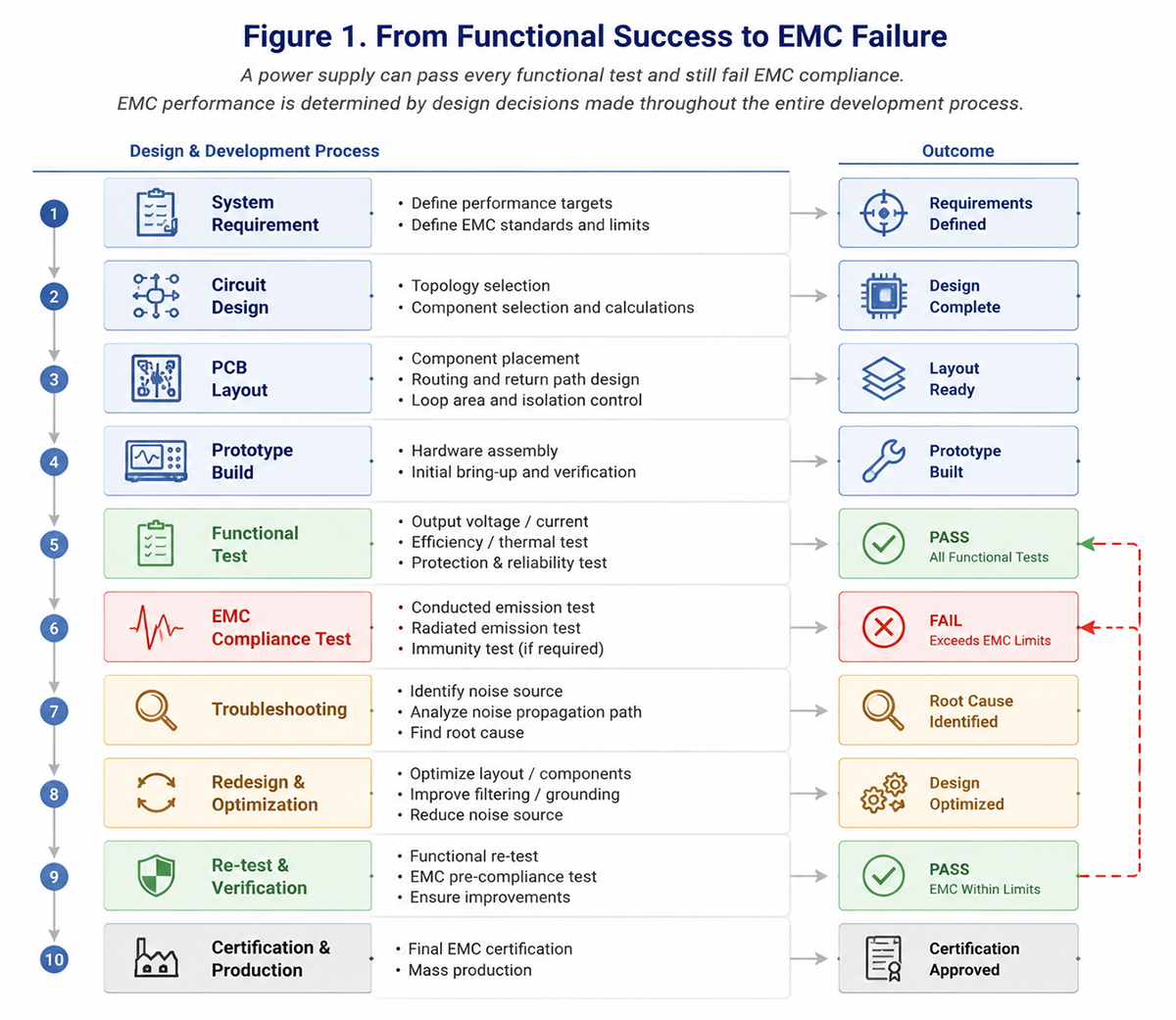
Figure 1. A power supply can operate correctly while failing EMC requirements because electrical performance and electromagnetic behavior are different design challenges.
Where Should Engineers Look First?
Common EMI sources include:
Switching Devices
Fast voltage transitions create high-frequency noise.
Switching Current Loops
High di/dt current paths generate magnetic field radiation.
Transformers
Leakage inductance and parasitic capacitance create unwanted coupling.
EMI Filters
Incorrect selection or placement reduces filtering effectiveness.
Cables
Common mode current can turn cables into antennas.
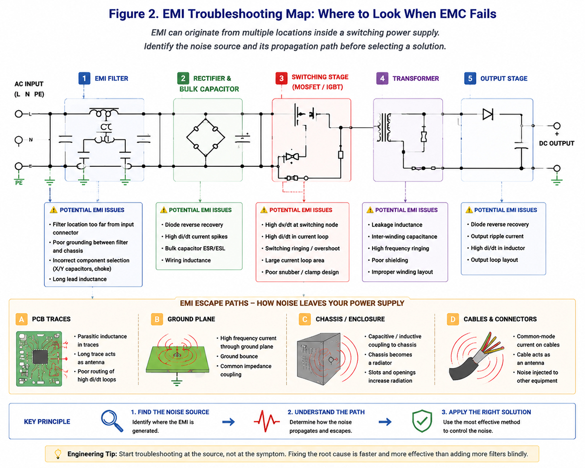
Figure 2. Identifying the noise source and propagation path is the first step toward an effective EMC solution.
Problem 1: Switching Loop Is Too Large
One of the most common EMC problems is poor control of the switching current loop.
The schematic may be correct.
The components may meet specifications.
However, PCB layout determines how electromagnetic energy behaves.
At high frequencies, PCB traces are not just connections.
They become part of the circuit.
A large switching loop creates:
· Higher parasitic inductance
· Voltage overshoot
· Ringing
· Increased EMI radiation
How to Improve It
Minimize High di/dt Loop Area
Keep switching paths short.
Place these components close together:
· Switching device
· Input capacitor
· Transformer or inductor
Control the Return Path
High-frequency current always requires a return path.
If uncontrolled, noise may flow through:
· Ground planes
· Signal traces
· Chassis
· Cables
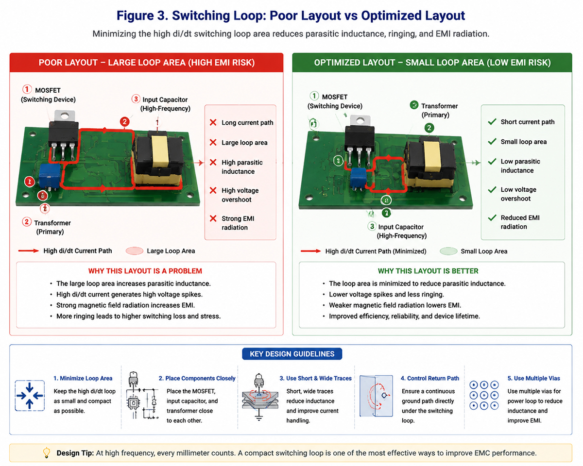
Figure 3. Minimizing high-frequency switching loop area reduces parasitic inductance and helps lower EMI radiation.
Design Tip
When troubleshooting EMC failures, find the high di/dt loop first.
Part 2
Reduce EMI Through Better Design
Once the EMI source has been identified, the next step is to apply targeted design improvements.
The most effective EMC solutions do not come from simply adding more components.
They come from understanding:
· Where noise is generated
· How noise propagates
· Which design method can control it
A practical EMC improvement strategy focuses on three areas:
1. Reduce noise at the source
2. Optimize filtering performance
3. Control unwanted propagation paths
1. Optimize EMI Filtering Based on the Noise Path
EMI filters are often the first solution engineers consider after an EMC failure.
However, a filter only works effectively when it addresses the actual noise path.
Increasing capacitor values or adding larger inductors does not always improve EMC performance.
The first step is understanding the dominant noise mechanism.
Differential Mode Noise
Differential mode noise flows between power conductors.
Typical sources include:
· Switching current ripple
· Input current pulses
· Rectifier switching behavior
Common solutions:
✓ X capacitor optimization
✓ Differential filtering
✓ Reduced input current ripple
Common Mode Noise
Common mode noise flows through unintended paths caused by parasitic coupling.
Typical paths include:
· Transformer capacitance
· Chassis
· Ground structures
· External cables
Common solutions:
✓ Common mode choke
✓ Y capacitor optimization
✓ Shielding and grounding improvement
Engineering Note
Different noise mechanisms require different solutions.
A larger filter does not always mean better EMC performance.
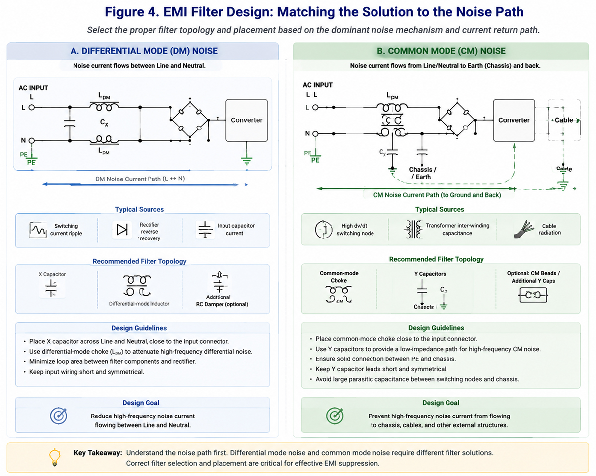
Figure 4. Effective EMI filtering starts with identifying the noise path. Differential mode and common mode noise require different suppression methods.
EMI Filter Design Considerations
Place the Filter Correctly
Even a well-designed filter can become ineffective if it is located incorrectly.
The EMI filter should be:
· Close to the power entry point
· Physically separated from switching noise sources
· Designed with a controlled return path
The goal is to prevent noise from entering or leaving the system.
Separate Clean and Noisy Areas
A good EMC design separates:
Noisy side
from
Clean side
Poor PCB arrangement can allow noise to bypass the filter through:
· Ground planes
· Copper areas
· Mechanical structures
Filter design and PCB layout must work together.
Design Tip
Do not design an EMI filter only from the schematic.
Always consider the complete current path, including PCB layout.
2. Reduce Switching Noise at the Source
EMI filtering reduces noise.
However, reducing noise generation at the switching source is often more effective.
The switching stage is usually one of the strongest EMI sources inside a converter.
Fast switching transitions and parasitic effects can create:
· Voltage overshoot
· Ringing
· High-frequency oscillation
These unwanted waveforms increase electromagnetic emissions.
Measure Before Modifying
Before adding suppression components, engineers should evaluate the switching waveform.
Important parameters include:
· Overshoot voltage
· Ringing amplitude
· Ringing frequency
· Oscillation duration
The waveform provides direct information about unwanted switching energy.
Common Optimization Methods
Reduce Parasitic Inductance
Improve:
· Switching loop layout
· Component placement
· Transformer connection design
A smaller current loop reduces unwanted stored energy.
Optimize Snubber and Clamp Circuits
Possible solutions include:
· RC snubber
· RCD clamp
· Active clamp
The goal is not simply reducing switching speed.
The goal is controlling switching energy while maintaining efficiency.
Balance Efficiency and EMC
Faster switching edges may improve efficiency.
However, extremely fast transitions can increase EMI.
Good design requires balancing:
· Switching loss
· Thermal performance
· EMC performance
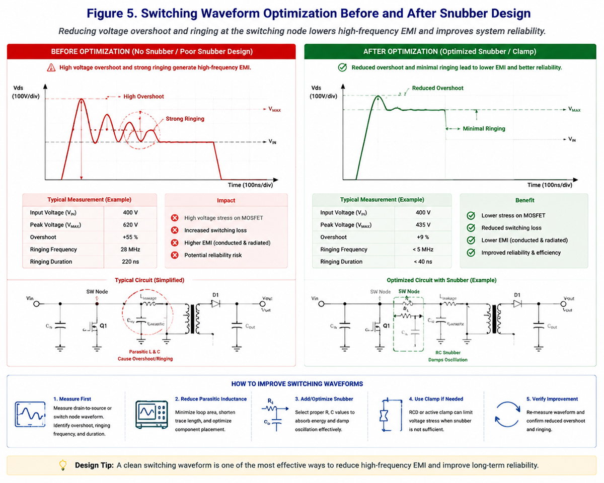
Figure 5. Controlling switching waveform quality reduces unnecessary high-frequency energy and improves EMC performance.
Engineering Note
Switching ringing is not only a reliability issue.
Every unwanted oscillation is also a potential EMI source.
3. Control EMI Escape Paths
Reducing noise generation is important.
But controlling how noise leaves the system is equally critical.
A noise source inside the converter does not automatically create an EMC failure.
The problem occurs when the noise finds an unintended path.
Common escape paths include:
· PCB traces
· Ground connections
· Chassis
· Input cables
· Output cables
Control High-Frequency Return Paths
At high frequency, current follows impedance—not simply the shortest visible connection.
Engineers should evaluate:
· Where high-frequency current returns
· Ground impedance
· Chassis connection points
· Separation between noisy and sensitive circuits
Manage Cable Radiation
External cables can become antennas when common mode current flows through them.
Practical improvements include:
✓ Optimized cable routing
✓ Controlled cable length
✓ Improved shielding connection
✓ Common mode suppression when required
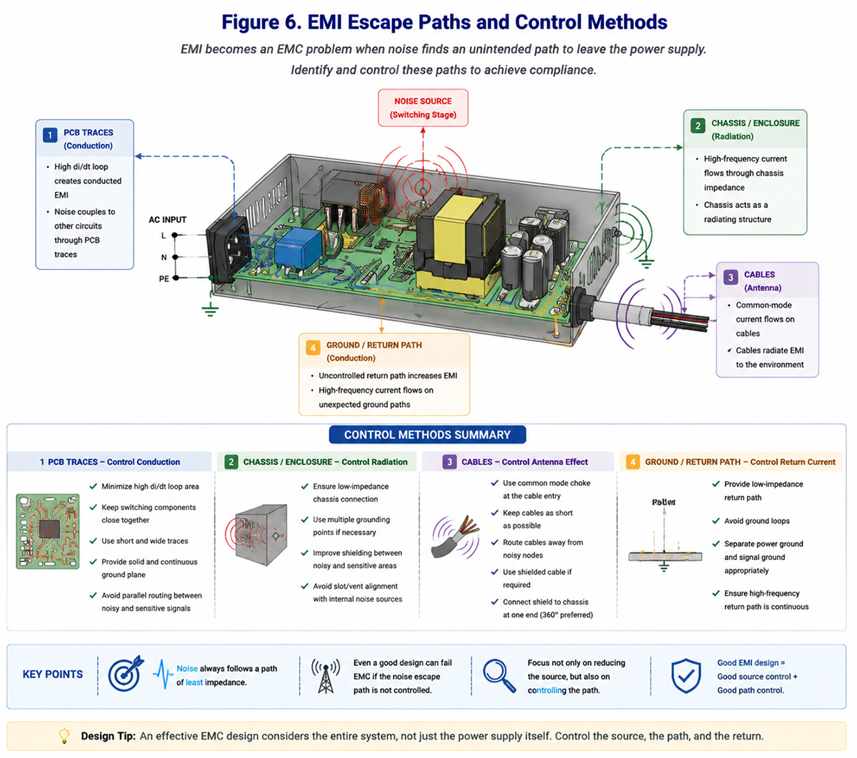
Figure 6. EMC problems occur when unwanted electromagnetic energy finds a path to escape the power supply. Controlling propagation paths is essential for compliance.
Design Tip
The best EMC solutions do not only reduce noise.
They control where the noise is allowed to flow.
Part 2 Summary
After identifying the EMI source, engineers should focus on three actions:
1. Match the filter to the noise mechanism
Understand the noise path before changing components.
2. Reduce noise at the switching source
Control:
· Overshoot
· Ringing
· High-frequency energy
3. Control propagation paths
Prevent noise from reaching:
· Cables
· Chassis
· External systems
Effective EMC design is not about fighting noise after failure.
It is about controlling electromagnetic energy from the beginning.
Part 3
Prevent EMC Failure Before Certification
Passing EMC testing should not depend on last-minute modifications in the laboratory.
Many EMC failures are discovered too late—not because the design cannot be improved, but because EMC performance was considered only after the prototype was completed.
At that stage, changes may affect:
· PCB layout
· Mechanical design
· Thermal performance
· Production schedule
A better approach is to treat EMC as a design requirement from the beginning.
1. Consider EMC During the Design Stage
EMC performance is influenced by decisions made before the first prototype.
During design review, engineers should evaluate:
· Where high-frequency current flows
· Where noise is generated
· How noise returns
· How noise may escape from the system
Switching Stage Review
Check:
✓ Is the high di/dt loop minimized?
✓ Are switching components placed close together?
✓ Is the high-frequency return path controlled?
✓ Are switching nodes separated from sensitive circuits?
Transformer Review
The transformer can become an important noise coupling path.
Engineers should consider:
✓ Leakage inductance
✓ Inter-winding capacitance
✓ Primary-to-secondary coupling
✓ Shielding requirements
EMI Filter Review
Before selecting filter components, verify:
✓ The dominant noise mechanism is understood
✓ Filter location is optimized
✓ Clean and noisy areas are separated
✓ Return paths are controlled
2. Perform Pre-Compliance Testing Early
Waiting until the final certification test creates unnecessary risk.
Pre-compliance testing helps engineers identify:
· Dominant emission frequencies
· Main noise sources
· Propagation paths
· Effectiveness of design changes
The goal is not to replace certification testing.
The goal is to reduce uncertainty before certification.
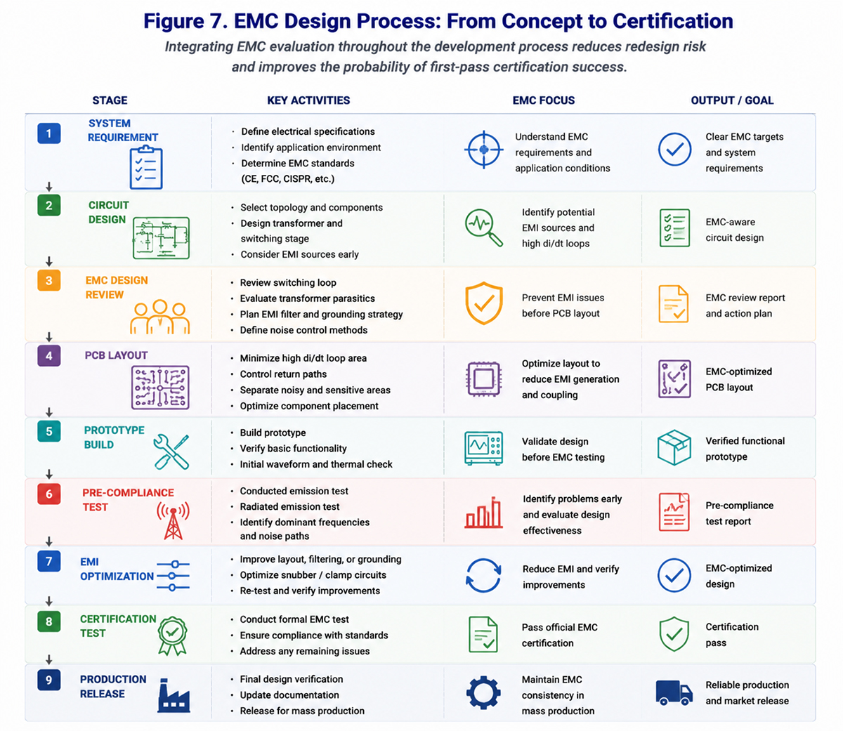
Figure 7. Integrating EMC evaluation throughout the development process reduces redesign risk and improves the probability of first-pass certification success.
3. EMC Is a System-Level Requirement
A power supply rarely operates alone.
In real applications, it works together with:
· Controllers
· Sensors
· Communication systems
· Industrial equipment
· Automation systems
A power supply may function correctly while still affecting system reliability if electromagnetic noise is not controlled.
Therefore, EMC is not only a certification requirement.
It is a system reliability requirement.
Final EMC Checklist Before Certification
Before submitting a power supply for EMC testing, engineers should review the following items.
Switching Stage
☐ High-frequency switching loops are minimized
☐ Switching waveform overshoot and ringing are controlled
☐ Snubber or clamp circuits are evaluated
☐ Switching harmonics are considered
PCB Layout
☐ High di/dt current paths are minimized
☐ Switching nodes are separated from sensitive circuits
☐ High-frequency return paths are controlled
☐ Grounding strategy is clearly defined
EMI Filter
☐ Noise type has been identified
☐ Differential mode and common mode noise are evaluated separately
☐ Filter components match the actual noise mechanism
☐ Filter placement is optimized
Transformer and Isolation
☐ Leakage inductance is controlled
☐ Parasitic capacitance is evaluated
☐ Shielding requirements are reviewed
☐ Unwanted coupling paths are minimized
Cable and System Integration
☐ Cable routing is reviewed
☐ Common mode current is controlled
☐ External cables are not becoming unintended antennas
☐ Chassis and grounding strategy are verified
Pre-Compliance Verification
☐ Conducted emissions are measured
☐ Radiated emissions are evaluated
☐ Critical frequencies are identified
☐ Design improvements are verified before certification
Final Thoughts
An EMC failure does not always mean the power supply design is fundamentally wrong.
In many cases, the converter already performs its primary electrical function correctly.
The challenge is controlling the electromagnetic energy created during switching operation.
A reliable EMC strategy follows four steps:
Find the noise source.
Understand the propagation path.
Apply the correct design solution.
Verify performance before certification.
By considering EMC throughout the development process, engineers can reduce redesign cycles, shorten certification time, and create more reliable power solutions.
BETTPOWER Engineering Support
At BETTPOWER, we understand that a power supply is more than a voltage conversion device.
A successful power solution must deliver:
· Stable electrical performance
· Reliable operation
· Efficient power conversion
· EMC compatibility
Through engineering-focused design and application support, BETTPOWER helps customers develop power solutions that meet both application requirements and compliance expectations.

Tel:020-32166196
Email:info@bettpower.com
Address:Building A1, No.1 Doutang Road, Huangpu District, Guangzhou City, Guangdong Province
- Product
- AC/DC Power Module
- DC/DC Power Module
- Support
- Application
- Sample Request
 WeChat
 Sample
 Tel
Tel
 Email
Email
 TOP
TOP